I wrote this article a couple months ago and I haven’t shared a piece like this on X for a while. So I thought i’d share it here as I know there are still lots of people that want to learn more about this industry!
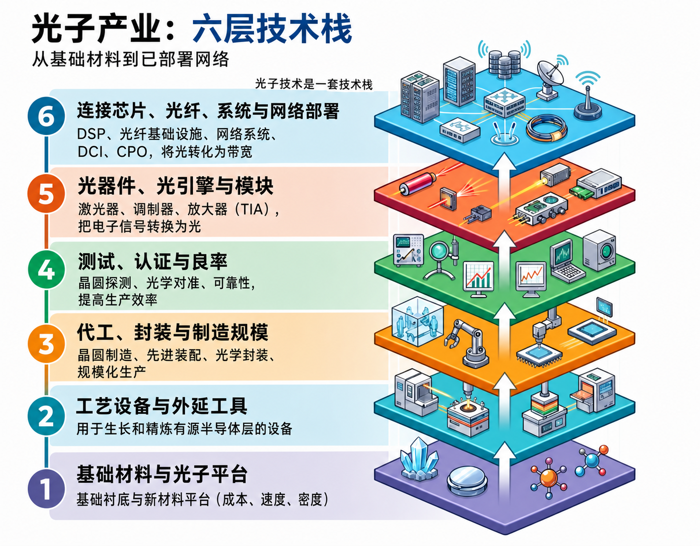
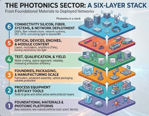
A laser, a photonic chip, a finished module, and a deployed network sit at different points in one long chain.
Some names supply the starting materials.
Some sell the tools used to grow and build devices.
Some handle fabrication, packaging, and scale-up.
Some solve test and yield problems.
Some build the optical engines, lasers, drivers, and modules.
Others provide the connectivity silicon, fiber, and network systems that turn light into usable bandwidth.
Grouping the sector correctly helps enormously. A substrate supplier, a transceiver vendor, a burn-in vendor, and a network systems vendor can all ride the same optical buildout while getting paid for entirely different reasons and on different timelines.
This framework breaks the trade into six layers from start to finish.
I have made several posts like this on X in the past, but I wanted to update the framework in a way that I hope is clearer and more useful for us.
If you read this article, you should come away with a stronger understanding of the major companies I track, what they do, and where they fit in the sector. There are plenty of other names that belong somewhere in this chain, especially international ones. Covering every company in the world would turn this into a directory instead of an article. If there is a company you want mapped into the framework, drop it in the comments.
Epitaxy: the growth of ultra-thin semiconductor layers with tight control over thickness and composition.
Foundry: a manufacturer that fabricates chips for customers.
Packaging: the work required to turn a chip or device into a usable part inside a real product.
Yield: the share of devices that work well enough to sell.
DSP: digital signal processor. In optics, a DSP cleans up and manages very high-speed data signals.
SerDes: serializer/deserializer. It moves data between parallel formats and very high-speed serial formats.
TIA: transimpedance amplifier. A TIA helps turn the weak current from a photodiode into a usable signal.
EML: electro-absorption modulated laser. A common high-speed optical device used in data center and telecom links.
DCI: data center interconnect. The links that connect one data center to another.
CPO: co-packaged optics. Optical components sit very close to the switch or accelerator package to improve bandwidth and power efficiency.
LPO: linear pluggable optics. A lower-power optical module design that reduces DSP work inside the module.
Layer 1: Foundational materials and photonic platforms#
This layer sits at the base of the stack. These names supply starting materials for photonic devices or develop new material platforms that could improve cost, speed, density, power, or manufacturability. When the material stack gets tight, every layer above it feels the pressure. We have already seen this layer act as a choke point for the rest of the industry.
AXT makes compound semiconductor substrate wafers, with indium phosphide (InP), gallium arsenide, and germanium as the main products. For photonics, InP carries the most weight because many high-performance optical devices for telecom and data center connectivity start there.
AXT sells the wafer while other layers sell the laser, the module, or the network. That makes AXTI an upstream way to follow optical demand, especially when the discussion shifts toward InP supply, capacity, or geopolitics. When substrate availability tightens, pricing power and delivery times can ripple upward through the chain. That dynamic can turn an otherwise invisible materials name into a meaningful choke point.
Aeluma is a platform story first. Their work centers on combining compound semiconductor performance with large-diameter silicon manufacturing, an approach that could improve how future optoelectronic devices scale in data center optics, sensing, quantum, and defense.
The core bet is the manufacturing platform itself. If it reaches commercial scale, ALMU could change the cost and manufacturability profile of future photonic devices. The angle is less about shipping standard optical parts into an established chain and more about shifting where that chain can go next, creating a different kind of upside in platform adoption, design wins, and eventual qualification.
Lightwave Logic fits best as a platform name with a differentiated technical angle. Their main asset is electro-optic polymer technology aimed at improving optical modulation, the process of encoding data onto light.
The upside comes from platform adoption inside future optical designs. The pitch ties directly into one of the central pressures inside AI infrastructure: higher bandwidth with tighter power budgets. If electro-optic polymers gain traction, LWLG could slot into modulators and interconnect architectures where speed and efficiency carry a premium.
IQE sells epitaxial wafers, adding the active semiconductor layers that sit on top of the starting substrate and later become part of lasers, detectors, and sensing devices. That places IQE between the raw wafer material and the finished optical device.
IQE gives us exposure to a key handoff point from materials to hardware. Their work ties into communications infrastructure, advanced sensing, and newer optical interconnect opportunities. In this framework, IQE helps show that a large part of the value chain is created before a finished device even exists.
After the substrate and material platform are chosen, the next step is building the active semiconductor layers that later become the laser, detector, or sensing device. This layer covers the tools used to grow and refine those layers.
Two core growth methods sit at the center here. MOCVD (metal-organic chemical vapor deposition) is widely used for scalable compound semiconductor production. MBE (molecular beam epitaxy) is used where tighter control over the crystal structure and layer stack carries more weight. Both shape film quality, yield, and how far a photonics platform can scale.
AIXTRON sits on the MOCVD side of this layer. Their systems are used to grow compound semiconductor structures across gallium arsenide and indium phosphide material systems, which feed directly into lasers and other photonic devices.
That places AIXA close to the factory buildout stage of the trade. When customers add optical manufacturing capacity, AIXA captures the equipment side of that expansion. In this framework, AIXA gives us exposure to the growth tools that help turn photonics demand into real production capability.
RIBER represents the MBE side of the layer. Their systems are built for highly controlled compound semiconductor growth, which is especially useful in optoelectronics, advanced research, pilot lines, and specialized production flows where the material stack itself carries enormous importance.
RIBER fits this framework as a precision-growth name. Where AIXA leans toward scalable MOCVD production, RIBER leans toward exact control at the epitaxy stage. That gives us a clean way to separate two very different growth-tool exposures inside the same photonics chain.
Veeco spans both MOCVD and MBE, giving VECO exposure to the two main epitaxy approaches used across compound semiconductors. VECO also sells process tools tied to adjacent manufacturing steps, which gives VECO a wider footprint across the buildout of advanced photonic devices.
On the photonics side, VECO’s Lumina MOCVD platform is designed for arsenide- and phosphide-based devices including VCSELs, edge-emitting lasers, and silicon photonics-related applications. VECO also maintains a full MBE portfolio, so VECO sits in a broader position than a single-method tool vendor.
Layer 3: Foundries, packaging, and manufacturing scale#
This is where photonics moves from lab success to commercial scale. A design can perform beautifully and still struggle once volume, packaging, and cost enter the picture. This layer covers foundries, advanced assembly, optical packaging, and broader manufacturing infrastructure.
Tower is one of the clearest foundry names tied to silicon photonics, with platforms addressing transceivers and other emerging photonic applications. TSEM has discussed production on 1.6T silicon photonics transceivers, placing TSEM right in the middle of one of the most active current demand cycles.
Foundry capability often decides which photonic ideas move beyond prototypes and into repeatable volume. TSEM gives customers access to mature process infrastructure without forcing each one to build that capability independently. That makes TSEM an important industrial base name inside the stack.
Fabrinet is one of the clearest manufacturing names in the optical sector and stands among the largest manufacturers of optical transceivers. Their position captures value in the part of the chain where precision packaging, alignment, integration, and scale all come together.
FN also carries a broad view across customers and product cycles without depending on a single device architecture. That supports resilience when volume ramps across multiple programs at the same time. In this framework, FN represents the manufacturing muscle required to turn optical designs into shipped hardware.
Sanmina helps move optical hardware from design into volume production. Their communications and optical businesses include custom optical transceivers, modules, subsystems, and broader networking hardware, along with the design, manufacturing, and test capabilities needed to build them at scale.
The angle here is industrialization. SANM supports process development, assembly, and test across the path from component work to finished systems, while customers retain the product IP. That gives SANM a reseat in the part of the photonics trade where hardware has to become repeatable, manufacturable, and ready for deployment.
This layer deserves far more attention than it typically gets. We have started to see that play out over the last couple of months. Photonics lives or dies on repeatability, reliability, and throughput. Wafer probing, optical alignment, burn-in, automated test, and system validation all sit here, and this layer helps decide whether a photonics story can turn technical promise into commercial economics.
Wafer-level burn-in is increasingly relevant for silicon photonics and optical I/O, and AEHR has become an important name in that process. Burn-in means stressing devices before final packaging so early failures show up sooner and at lower cost.
AEHR has won and expanded business tied to silicon photonics transceivers and optical interconnect applications for AI data centers. Catching failures earlier saves time, money, and packaging effort later, and that becomes even more valuable as optical content rises and qualification pressure increases alongside it.
Wafer-level optical probing has become a real bottleneck in photonics, and FORM sells dedicated silicon photonics test solutions with expanded capabilities through the acquisition of Keystone Photonics.
Photonic chips are harder to test than ordinary electrical chips because light and electricity have to be measured together. FORM brings repeatability and automation to that process, sitting close to one of the least glamorous yet most decisive parts of photonics manufacturing. Without dependable wafer-level test, scale-up slows and costs rise quickly.
COHU is broader and not photonics like AEHR or FORM, yet COHU still belongs in the map. Their focus on semiconductor test, handling, inspection, and interface products extends into optoelectronics and optical-sensor exposure.
The relevance shows up in the physical movement, screening, and validation of devices as production scales. It is a quieter contribution, yet it still touches the real economics of manufacturing throughput and finished-device quality.
TER already has a massive automated test footprint across semiconductors, and Photon 100 extends that footprint directly into silicon photonics and co-packaged optics. Photon 100 targets high-volume optical test across wafer, optical engine, and module stages, giving TER direct exposure to one of the hardest parts of scaling advanced optical hardware.
As optical hardware gets denser and moves closer to switches and accelerators, customers need fast, repeatable test at manufacturing scale. That is exactly where TER sits. TER brings a large established test base into a newer optical market where yield, speed, and consistency can shape who ramps cleanly.
VIAV sits a little differently from the other names in this layer because their work spans both semiconductor-adjacent validation and high-speed network and system validation.
VIAV has launched 1.6T Ethernet and AI-infrastructure test solutions, giving VIAV exposure to the later stages of the chain where advanced optical hardware has to prove itself before broad deployment. Their role is especially useful when tracking the transition from component readiness to network readiness, covering link assurance, field validation, and system-level confidence.
Layer 5: Optical devices, engines, and module content#
This is the hardware heart of the trade. These names make the optical guts of the link: lasers, detectors, optical engines, drivers, TIAs, and modules. This is where electrical signals become light and then turn back into electrical signals again. The names can look similar on the surface while carrying very different levels of vertical integration and manufacturing control.
Lumentum sits deep in data-center optics through EMLs, CW lasers, optical transceivers, optical circuit switches, and ELSFP modules for CPO. That product set covers several key parts of the link at once: the laser source, the pluggable module, the optical switching layer, and the external-light-source path being built around silicon photonics and CPO.
LITE participates in current high-speed optical links while also carrying leverage to architecture changes around optical switching and centralized light sources. That makes LITE one of the fuller expressions of the data-center optical hardware layer.
Coherent reaches across the optical communications stack through communication components, integrated sub-assemblies, datacom transceivers, and optical circuit switches. Their datacom portfolio spans a wide range of transceiver formats and speeds, while the communications component lineup includes photodetectors, receivers, pump lasers, passive components, and integrated optical assemblies.
That combination gives COHR exposure to the building blocks, the assembled hardware, and the switching layer across several optical designs and several points in the same link budget. Breadth is the core of the story here.
AAOI starts with lasers and laser components, then builds upward through components, subassemblies, and complete products. AOI describes itself as a vertically integrated supplier with in-house design and manufacturing spanning semiconductors, laser components, and optical transceivers.
Starting at the laser layer and finishing at the transceiver gives AAOI a tighter link between component content and module revenue. That makes AAOI a direct way to follow transceiver ramps with deeper internal exposure to the hardware inside them.
POET builds optical engines and related products around the Optical Interposer platform, with a pitch centered on integrating electronics and photonics in a way that reduces traditional assembly, alignment, and testing complexity.
The value proposition comes from making optical products easier and cheaper to build, which can become especially attractive in a market where packaging and alignment costs keep rising with speed and density. POET represents a design approach aimed at simplifying the build itself rather than competing on one isolated device.
The photonics business at SIVE centers on high-power indium phosphide laser chips and arrays for data center optical interconnects, explicitly targeting pluggable modules, silicon photonics platforms, and CPO-type designs.
SIVE provides active optical content at the laser-source level, a role that could grow in importance as future optical systems rely more heavily on external or remote light sources. SIVE sells a critical ingredient that other architectures depend on, which gives the name leverage to shifts in system design even without owning the full finished product.
MACOM supplies the high-speed analog and mixed-signal semiconductors that sit inside optical links, including modulator drivers and related signal-chain content. Their roadmap includes 448G-per-lane drivers for 3.2T connectivity, with products tied to SiPh, EML, and TFLN modulator platforms.
MTSI belongs in this layer because the optical bill of materials extends well beyond lasers and photodiodes. The analog and mixed-signal content inside the link helps determine signal integrity, lane speed, and overall optical-engine performance. As architectures move toward 224G and 448G per lane, that electronic layer carries more weight.
Layer 6: Connectivity silicon, fiber, systems, and network deployment#
This is where photonics becomes working infrastructure. These names may sit farther from the laser itself, yet they remain essential because they provide the DSPs, connectivity silicon, fiber, transport systems, and network architectures that allow optical bandwidth to scale across real environments.
Credo has expanded well beyond a cable-and-SerDes framing toward a broader connectivity platform. CRDO sells ZeroFlap optical transceivers and has agreed to acquire DustPhotonics, which brings silicon photonics photonic integrated circuit technology deeper in-house.
That broadening of scope is significant because AI fabrics increasingly reward vendors that can control more of the link. CRDO shows how a connectivity name can grow deeper optical exposure over time rather than starting as a pure photonics story from day one.
Modern optical links increasingly depend on advanced DSPs, PAM4 connectivity, and co-packaged architectures that MRVL helps define. Their major optical DSP products and public commentary around co-packaged optics for AI infrastructure place MRVL near several of the biggest architecture decisions in AI networking.
As bandwidth climbs and co-optimization between optics and electronics grows more consequential, MRVL’s influence inside the stack increases. MRVL represents the silicon brain behind much of the optical plumbing.
SMTC sells the analog chips that sit inside high-speed optical links, especially TIAs and laser drivers used in 800G and 1.6T modules, with newer products aimed at 224G-per-lane systems and future 3.2T designs.
That places SMTC inside the part of the link where power, signal integrity, and lane speed all start to tighten. As optical links move to higher speeds, cleaner signal paths and lower power per bit become more important, especially in architectures like LPO, NPO, and CPO.
CIEN monetizes bandwidth once traffic is moving across optical networks. Their business includes coherent optics, DCI, transport systems, automation software, and broader network architecture.
The role becomes more visible as AI traffic pushes higher-capacity links between buildings, campuses, and regions. CIEN helps show that the photonics trade extends beyond components and into the systems carrying long-haul and inter-data-center traffic.
NOK carries growing exposure to AI data center networking and optical DCI through switching, routing, automation, coherent optics, and optical transport platforms.
Their role sits closer to how networks are deployed, managed, and extended across real environments, creating a different kind of exposure from the device vendors earlier in the stack. NOK shows how the photonics trade reaches all the way into system architecture and network control.
Corning is the bridge name in this framework. At a deep level, GLW is a materials science leader, and in the public market their role in this trade shows up most clearly through fiber, cable, and connectivity products that allow dense AI networks to get built.
Dense optical networks require enormous amounts of physical fiber infrastructure, and GLW captures that side of the buildout directly. AI networking still has to travel through real glass in the real world, which makes GLW a useful bookend to a stack that begins at the wafer and ends at the deployed link.
The information provided is for informational purposes only and does not constitute investment advice, a recommendation, or an offer to buy or sell any securities. The author may hold a position in the securities mentioned. Readers should conduct their own due diligence and consult with a financial advisor before making investment decisions.