Why would Intel, a foundry, hire the former CEO of a memory company like SK Hynix?
Not to break into the HBM business. Seok-hee Lee reports directly to Lip-Bu Tan, overseeing advanced packaging, system integration, and back-end process and manufacturing. One phrase deserves your attention: advanced packaging.
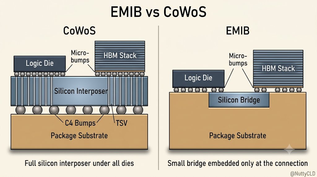
If you’ve followed Intel for a while, you’ll remember the EMIB-versus-CoWoS war. EMIB (Embedded Multi-die Interconnect Bridge) skips the full silicon interposer that CoWoS lays down, and instead buries a small silicon bridge only where two dies need to connect.
Round one went to CoWoS. Flagship GPUs from Nvidia and AMD wanted maximum bandwidth and minimum latency, and EMIB, limited by the bridge’s area and routing density, couldn’t keep up. It lost the socket. After that, EMIB lived mostly inside Intel’s own CPUs. The technology didn’t fail. It lost the fight to become the GPU standard.
Then the game changed.
In 2026, the bottleneck isn’t the wafer. It’s the package. CoWoS is capacity-short and, thanks to that large interposer, expensive. EMIB walks straight into the gap. Put the bridge only where you need it, and you get a cheaper package, freedom from reticle-size limits, and an edge on large multi-die designs. Google is evaluating EMIB for its 2027 TPU v9, and Meta is weighing it for MTIA. The explosion of custom ASICs and inference accelerators is EMIB’s stage.
Intel won’t beat TSMC at the leading node anytime soon. But packaging is a younger layer, less locked in, and above all, something Intel is genuinely good at. If there’s a front where Intel can land a blow on TSMC, it’s packaging, not the node.
In that light, hiring SK Hynix’s former CEO reads as a challenge aimed squarely at TSMC, which holds the heart of GPU-plus-HBM integration. The hardest part of AI packaging is HBM integration and mass-producing it at high yield, and Lee is the man who pulled exactly that off in the HBM era. Spin packaging out as its own business unit reporting straight to the CEO, and the org chart becomes the statement of intent.
Of course, the CoWoS-locked volume at Nvidia and AMD won’t move overnight. But the direction is unmistakable: make packaging a standalone weapon.
So here’s the picture. TSMC’s real moat isn’t the leading node alone. It’s the node-plus-CoWoS bundle: the AI accelerator and its HBM coming from a single house. What Intel’s next-generation packaging is after is breaking that bundle apart. TSMC’s base die, SK Hynix’s DRAM, someone else’s logic. Wherever each piece is made, Intel does the final integration. That’s the goal.
Figure 1: CoWoS uses a full silicon interposer under all dies; EMIB embeds a small bridge only at the connection.