
推理芯片架构图谱:三类瓶颈与十二家公司
目录
摘要#
核心问题#
推理芯片初创公司不能只按速度排名。文章用三个相互连接的瓶颈重新划分市场:存储带宽、计算灵活性的成本,以及部署与功耗。存储放在哪里,决定芯片能承载多大的模型和计算方式能保留多少灵活性;这两项选择又进一步决定产品必须以单芯片、知识产权授权还是机架系统的形式出售。
四类架构路线#
- 以 SRAM 为中心:Groq 用 230MB 片上 SRAM 与确定性数据流追求低延迟;Cerebras 用整片晶圆上的 44GB SRAM 和 MemoryX 权重流处理大模型。优势是带宽与延迟,代价是容量、系统连接或执行方式受到约束。
- SRAM 加低成本 DRAM:d-Matrix 使用 2GB SRAM 加 256GB LPDDR5X,Tenstorrent 使用 GDDR6 和开放的 RISC-V 体系,主动绕开 HBM 供应、价格与 CoWoS 封装瓶颈。这条路线以更便宜的外部存储换取计算灵活性。
- 分层存储:SambaNova 把 SRAM、HBM 和 DDR 分成三级,Positron 则使用带 HBM 的 FPGA 再连接 DDR5。它们通过存储层级快速切换模型,更适合连续调用多个模型的智能体工作负载。
- 以 HBM 为中心:Rebellions、FuriosaAI、Etched 和 MatX 用大容量 HBM 支撑模型,并在 CGRA、张量收缩处理、专用 ASIC 与通用训练/推理之间作不同取舍。Etched 最接近硬连线极端,但其公开声明已把验证范围扩展到 DeepSeek、Qwen、Mamba 和 Llama,说明市场正迫使专用架构重新增加灵活性。
商业化与竞争边界#
大多数公司最终都趋向销售机架系统,因为客户需要可直接部署的基础设施,而不是一颗孤立芯片。Tenstorrent 是例外,它通过知识产权授权让客户拥有自己的芯片。文章认为,初创公司的生存空间夹在两股力量之间:英伟达通过 Vera Rubin、NVL72、HBM4、CUDA 和 NVLink Fusion 把竞争单位从芯片提升到整机架;谷歌 TPU、亚马逊 Trainium、微软 Maia 和 Meta MTIA 则从下方吸收各自云内的可预测推理负载。
关键公司与信号#
文章引用公司披露称,Etched 已完成台积电 N4P 首次流片、拥有逾 10 亿美元客户合同,并累计融资 8 亿美元;还提到英伟达对 Groq 技术的授权、Cerebras 上市以及高通洽购 Tenstorrent 等事件。这些数字和交易状态主要来自公司公告或媒体报道,部分尚未完成,不能视为独立验证的事实。
风险与不确定性#
私营公司的估值、技术指标和客户合同难以独立核实;首次流片不等于量产,后续仍有性能、良率、软件、客户验证和交付风险。专用芯片还面临模型架构快速变化的问题,而通用芯片则要承担更高的调度与软件开销。英伟达的软件生态和整机架集成,以及云厂商内部芯片对需求的吸收,都会压缩初创公司的可服务市场。
Takeaway#
比猜哪一家初创公司获胜更可靠的研究方法,是追踪所有架构共同依赖的底层需求:晶圆代工、SRAM/HBM/DDR、先进封装、互连、供电、散热和机架。不同路线只是把价值量导向不同环节;推理需求增长时,这些共同基础设施比单一公司名单更具持续性。
中文译文#
以下为 X 长文中公开显示部分的完整译文。Substack 后续章节见下一节“全文后半部分梳理”。
本文可在 Substack 免费阅读。
2026 年 6 月 30 日,沉寂两年多的 Etched 结束隐身状态。公司宣布,其基于台积电 N4P 制程的首颗芯片已成功完成 A0 流片,客户合同金额超过 10 亿美元,累计融资 8 亿美元,首批机架将于今年夏季出货。一家二十多个月未曾发声的公司,已经推进到可工作的芯片和机架级产品验证阶段。
类似的消息如今几乎每个季度都会出现。2025 年 12 月,据报道英伟达以约 200 亿美元的交易获得 Groq 推理技术授权,并吸纳其关键人员。2026 年 5 月,Cerebras 上市,首日盘中市值一度接近 800 亿美元。6 月又有报道称,高通正在洽购 Tenstorrent,交易估值约为 80 亿至 100 亿美元。
资本市场之所以押注推理芯片公司被收购或上市,是因为人工智能智能体的普及可能推动推理需求激增。但这并不是一场只凭速度就能排名的竞赛。即使同为推理芯片,存储放在哪里、计算功能固定到什么程度,以及销售芯片还是系统,都会彻底改变业务性质。每一种选择都针对英伟达无法高效覆盖的不同工作负载。
因此,正确理解这些公司,需要先看它们的技术选择,再看估值或速度。把初创公司的路线图,与英伟达及超大规模云厂商如何防守并侵入同一市场叠加起来,才能看清这些公司真正可能占领的空间。
本文首先把推理问题拆成三类瓶颈,并用可测量的规格说明 12 家公司如何回答每个瓶颈;随后按存储路线深入分析各类方案在实践中如何运作;最后讨论英伟达与超大规模云厂商如何从上下两端挤压市场,以及初创公司的真实生存空间。目标不是预测哪一家获胜,而是勾勒整场竞争将走向何处。
目录#
- 推理存在三类瓶颈
- 十二家公司如何应对这些瓶颈
- 深入分析四类阵营
- 英伟达与超大规模云厂商如何回应
免责声明#
本文依据公开材料与公司公告进行分析,不构成任何证券买卖建议。私营公司的估值和技术说法主要来自公司自身披露,往往难以独立验证。文中收购材料包含尚未完成的谈判。芯片规格取自各公司公开资料,并可能因代际和配置不同而变化。任何投资决策的责任完全由读者承担。
一、推理存在三类瓶颈#
训练和推理都属于人工智能计算,但计算性质完全不同。训练是在海量数据上一次性教会模型;推理则是持续运行已训练模型以生成 Token 的长期任务。
大多数新闻关注训练,真正持续产生费用的却是推理。每一次查询、每一次智能体调用,每天都在消耗电力和计算周期。随着编程智能体和自主智能体在 2025 年下半年普及,这种负担呈指数级增长。智能体会把任务拆成多个步骤,链式调用模型,并在每一步生成新的 Token,再把这些 Token 作为下一步输入。
推理芯片若要与 GPU 形成差异,就必须解决 GPU 在推理时遇到的问题。这些问题可以拆成三类瓶颈。
瓶颈一:存储带宽#
推理生成 Token 的解码阶段,每产生一个 Token,都要从存储器中重新读取整套模型权重。若每秒生成 10 个 Token,单个用户每秒就可能需要读取数 TB 的权重。在此期间,计算单元大部分时间处于空闲,整体性能取决于从存储器拉取数据的速度。
无论 FLOPS 多高,只要存储带宽不足就没有帮助。这就是“存储墙”,也是推理芯片设计最根本的约束。
瓶颈二:灵活性的成本#
GPU 为通用计算而设计。通用性的代价是,Transformer 推理会把计算周期消耗在指令获取、线程调度和内核启动等开销上,使许多推理工作负载的实际利用率远低于峰值性能。
硬件越针对特定工作负载固定,就越能减少这些浪费;但固定程度越高,能够运行的其他模型就越少。灵活性与效率彼此拉扯。
瓶颈三:部署与功耗#
无论芯片多快,如果无法装入数据中心机架,或者无法处理功耗和热量,就卖不出去。尤其是大模型往往需要多颗芯片,因此必须把它们连接起来。此时,芯片间互连、散热能力,以及能否在几天内部署到标准数据中心,都会决定产品的实际表现。
三类瓶颈并非彼此独立,而是顺序相连。瓶颈一中选择哪种存储,会限制瓶颈二,也就是可运行哪些模型以及能保留多少灵活性。单独使用 SRAM 速度快,却无法容纳大模型;加入 HBM 能提高容量,却要承担供应与封装负担。
这些选择形成的存储与计算结构,又会决定瓶颈三的系统设计:需要连接多少颗芯片,以及最终以何种产品形态销售。沿着这三个维度观察,12 家公司呈现的不是一份公司名单,而是一张设计哲学地图。
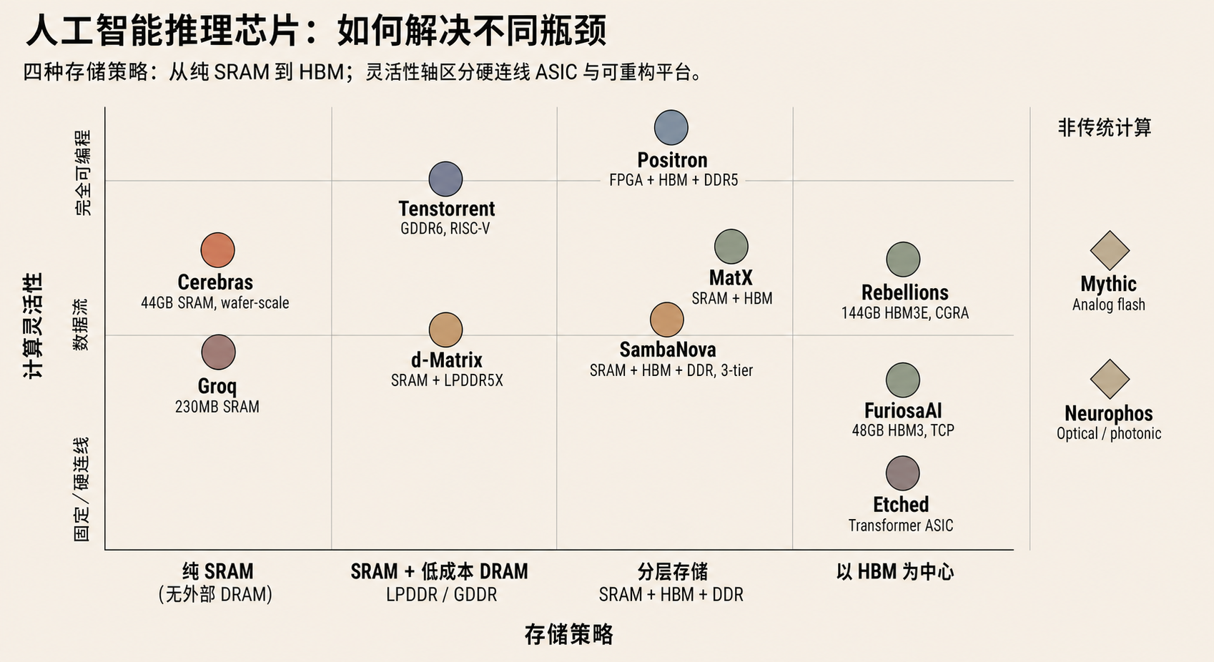
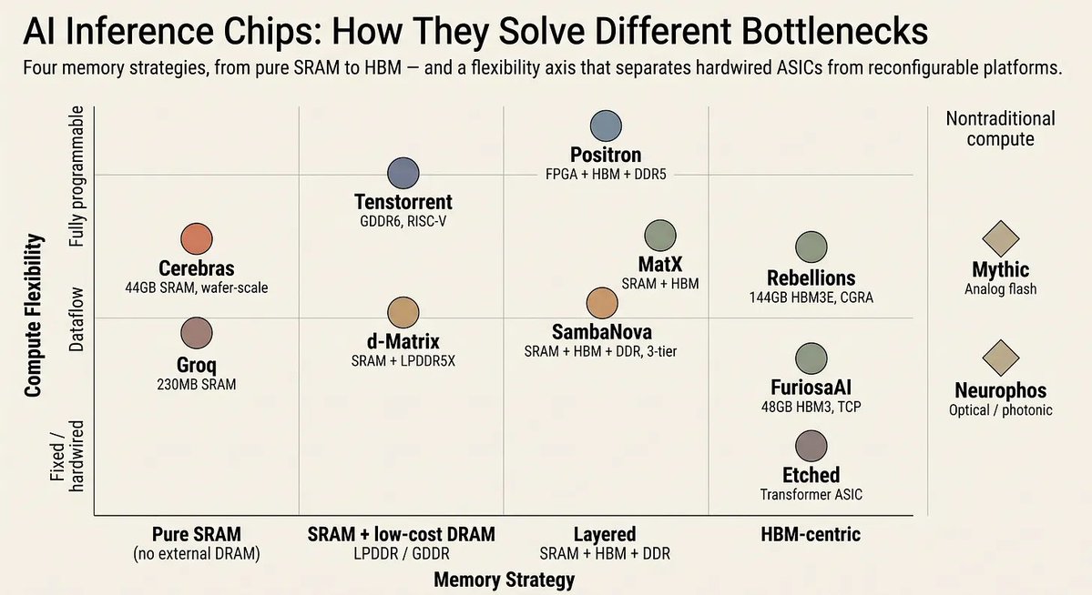
图 1:横轴为存储策略,纵轴为计算灵活性;不同公司在容量、带宽与可编程性之间作出不同取舍。
二、十二家公司如何应对这些瓶颈#
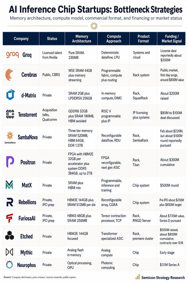
下表用公开规格列出各家公司对三类瓶颈的回答。状态栏区分已授权、已上市、处于收购谈判或仍为私营的公司,从而把已经退出或被大型公司吸收的项目,与仍独立经营的私营公司区分开来。
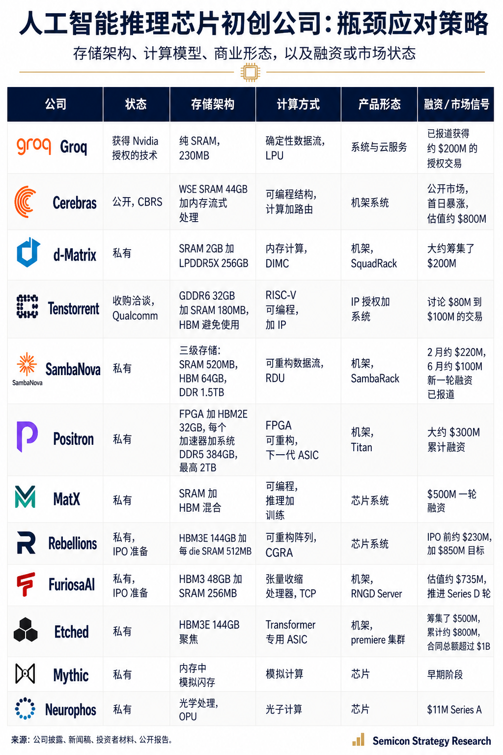
图 2:十二家公司的状态、存储架构、计算方式、产品形态和融资/市场信号。
这张表真正重要的不是公司名称,而是推理芯片市场并非单一市场。有些公司试图避开 HBM,有些公司反而更依赖 HBM;有些用 SRAM 把存储瓶颈拉进芯片内部,还有一些用 DDR 或 LPDDR 改变成本结构。
因此,竞争的关键与其说是谁比英伟达更快,不如说是谁能用更低成本,解决英伟达正在以昂贵方式解决的瓶颈。用这个视角阅读每一列,设计哲学的地图就会显现。
从瓶颈一的存储列由上往下看,可以看到推理芯片市场的基本结构。只有两种设计以 SRAM 为中心,尽量降低对 HBM 的依赖。Groq 与 Cerebras 共享这一理念,但实现方式不同。
Groq 在 230MB 片上 SRAM 上使用确定性数据流来降低延迟。Cerebras 则把 WSE 的 44GB SRAM 与基于 MemoryX 的权重流结合,以处理大模型。两者片上容量相差约 190 倍,因此路线也随之分化:Groq 的 SRAM 较小,运行大模型需要连接许多芯片;Cerebras 则把大模型放到单片晶圆上。
第二类方案仍使用 SRAM,但不用 HBM,而是用低成本 DRAM 补强容量。d-Matrix 把 256GB 通用 LPDDR5X 连接到 2GB 片上 SRAM,Tenstorrent 则使用 GDDR6。两者都在主动绕开 HBM 的供应紧张、高价格和复杂封装。Tenstorrent 首席技术官 Jim Keller 曾公开表示,只要使用 HBM,就无法击败英伟达。
第三类方案把 HBM 纳入分层结构。SambaNova 把 SRAM、HBM 和 DDR 分成三级,把多个模型保留在存储器中,并在毫秒级完成切换。Positron 则为已经带有 HBM 的 FPGA 再连接 DDR5。
第四类方案以 HBM 为中心。Rebellions 用 144GB HBM3E 获得大容量,FuriosaAI 则使用 48GB HBM3。值得注意的是,Rebellions 每颗裸片还带有 512MB 片上 SRAM,高于 FuriosaAI 的 256MB。即使同为 HBM 路线,不同公司的片上存储策略仍不相同。
从瓶颈二的计算列看,可以得到一条灵活性光谱。一端是 Etched,它把 Transformer 运算直接固定在硅片上的专用 ASIC。不过 Etched 在 6 月 30 日的公告中表示,客户验证范围已经超出最初的纯 Transformer 设计,扩展到 DeepSeek、Qwen、Mamba 和 Llama。Mamba 属于 SSM、DeepSeek 属于 MoE,它们的加入说明 Etched 支持的模型范围比最初的纯硬连线描述更广。
另一端是 Positron。FPGA 可以在物理层重新配置逻辑门,因此灵活性最高。两端之间依次存在可重构阵列(Rebellions 的 CGRA)、可重构数据流(SambaNova 的 RDU)、确定性数据流(Groq 的 LPU)和张量收缩处理(FuriosaAI 的 TCP)。
瓶颈三一列最显眼的事实是,几乎所有公司最终都趋向机架级系统。客户需要的是可以直接部署的基础设施,而不是单独一片硅,因此只卖芯片已经很难赢得市场。这也是大额融资集中在系统销售公司的原因。
Tenstorrent 是例外:它不销售芯片,而是把设计作为知识产权授权,让客户拥有自己的芯片。
本文可在 Substack 免费阅读全文。以下后续内容依据公开全文进行结构化梳理。
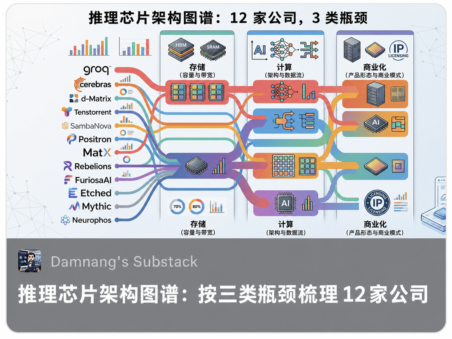
图 3:原文的 Substack 全文入口。
全文后半部分梳理#
三、深入分析四类阵营#
以 SRAM 为中心:Cerebras 与 Groq#
Cerebras 通过晶圆级集成,把整片 300mm 晶圆作为单颗芯片使用。WSE-3 在单芯片上放置 44GB SRAM,靠近计算核心,文章给出的带宽为每秒 21PB;大模型无法完全放入片上 SRAM 时,再通过 MemoryX 实时流入权重。其优势是无需把大模型拆到多颗芯片,也不必在 WSE 本体连接 HBM。
Groq 使用完全不同的路线:片上 SRAM 只有 230MB,却在编译阶段固定所有操作的顺序与时序,以确定性数据流消除运行时调度浪费,换取极低 Token 延迟。代价是运行大模型时必须把许多芯片连成系统。
文章认为,这一路线会把部分原本属于 DRAM 的需求,转移为逻辑晶圆中的 SRAM 面积,更直接利好晶圆代工。与此同时,把存储拉入芯片内部,往往也会迫使计算固定在特定执行方式上,因此灵活性较低。
SRAM 加低成本 DRAM:d-Matrix 与 Tenstorrent#
d-Matrix 的数字式存内计算把乘法器放入 SRAM 电路,在数据存储位置直接完成计算,以减少数据搬运;外接 256GB LPDDR5X,并使用有机基板,绕开 HBM 和 CoWoS。Tenstorrent 则使用 GDDR6、RISC-V Tensix 核心和知识产权授权模式。
这两家公司共同瞄准封装瓶颈:英伟达占据大量 HBM 与 CoWoS 产能,新进入者即使设计性能足够,也可能拿不到供应。若这条路线被验证,推理芯片需求并不会与 HBM 需求一比一增长;一部分增量会流向 LPDDR、GDDR、有机基板和标准封装。
分层存储:SambaNova 与 Positron#
SambaNova 使用 520MB 片上 SRAM、64GB HBM 和 1.5TB 外部 DDR:高频权重放 SRAM,当前模型放 HBM,待切换模型放 DDR,并以毫秒速度交换,适合频繁切换模型的智能体。Positron 第一代 Atlas 采用 FPGA,用较低效率换取快速上市,并把 FPGA 内置 HBM 与 DDR5 组合;下一步则是转向自研 ASIC Asimov。
这条路线的灵活性主要来自存储层级,而不是计算电路。一个芯片同时搭载 HBM 与 DDR,意味着推理普及可能同时拉动多类存储,而不是只增加 HBM。
以 HBM 为中心:Rebellions、FuriosaAI、Etched 与 MatX#
Rebellions 用 144GB HBM3E 和每颗裸片 512MB SRAM 配合可重构 CGRA;FuriosaAI 用 48GB HBM3、256MB SRAM 与张量收缩处理器,并以 LG 的 EXAONE 部署作为验证案例。Etched 把 Transformer 运算直接固化到 Sohu ASIC 中,追求极端效率;但其最新模型验证范围扩大,说明完全硬连线难以适应模型架构变化。MatX 同时面向训练与推理,但公开技术细节和基准较少,外界难以验证其估值。
文章的共同判断是:即便在 HBM 阵营内部,专用程度也在向中间收敛。完全通用会退化成 GPU 的高开销,完全固定又会被模型创新淘汰,因此更现实的方向是固定整体结构,同时保留参数和部分操作的可重构性。
四、英伟达与超大规模云厂商如何回应#
英伟达把竞争单位从芯片提升到系统#
英伟达的防守不是继续比较单芯片,而是把 GPU、Vera CPU、NVLink 6、网络与安全芯片整合进 Vera Rubin NVL72 机架。客户购买的是包含计算、存储、CPU 和网络的基础设施;竞争者若想替换其中一颗芯片,往往必须改变整套架构。
HBM4 提高带宽,CUDA 的二十年生态形成高切换成本,NVLink Fusion 又把外部 ASIC 纳入英伟达互连标准。对真正有差异化的技术,英伟达还可以通过授权和吸纳人才处理,Groq 就是文章举出的案例。
云厂商用内部芯片吸收需求#
谷歌 TPU、亚马逊 Trainium、微软 Maia 和 Meta MTIA 无需对外销售,因此不必建立说服外部客户的软件生态,也无需追求完全通用。它们可以直接吸收各自云内可预测的大规模推理负载,缩小留给外部芯片公司的市场。
但这些芯片通常绑定自有软件栈和云平台:Trainium 依赖 Neuron SDK,TPU 依赖 JAX/XLA,Maia 与 MTIA 也不向外部普遍出租。外部团队迁移时需要移植服务栈,并承担云锁定。因此,内部 ASIC 更适合可预测的大批量推理,而灵活训练、实验和通用租赁市场仍由英伟达主导。
结论#
完整市场有三层:底层是存储带宽、灵活性成本、部署与功耗三类约束;中层是 12 家初创公司的架构路线;上层则是英伟达的整机架与软件生态,以及云厂商内部 ASIC 的双重挤压。
作者认为,猜中哪一家初创公司最终获胜既困难,也不是最重要的问题。更确定的是所有方案都会经过晶圆、存储、封装、供电、散热和机架:SRAM 路线增加晶圆面积,避开 HBM 的路线带动 DDR/LPDDR 与标准封装,高密度路线增加功率和冷却需求。顺着不同架构追踪组件需求,比记住 12 家公司名称更持久。
原文(英文)#
原文标题(英文):The Inference Chip Architecture Map: 12 Companies Sorted by Three Bottlenecks 收录范围:X 长文中公开显示的前两节;后续全文见文中的 Substack 链接。
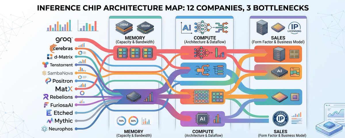
This article is available for free on Substack.
On June 30, 2026, Etched came out of stealth after more than two years of silence. The company reported a successful first silicon tapeout (A0) on TSMC’s N4P process, over a billion dollars in customer contracts, $800 million in cumulative funding, and first racks shipping this summer. A company that had said nothing for more than 20 months had moved to working silicon and rack-level product validation.
Announcements like this now arrive every quarter. In December 2025, Nvidia licensed Groq’s inference technology in a deal reported at roughly $20 billion and brought over its key people. In May 2026, Cerebras went public and touched nearly $80 billion in intraday market cap on its first day. In June, reports followed that Qualcomm was in talks to acquire Tenstorrent at $8 to $10 billion.
Behind this run of inference chip companies getting acquired and listed is a bet by capital markets that the spread of AI agents will drive a surge in inference demand. But this is not a race you can rank on speed alone. Even among inference chips, the character of the business changes completely depending on where you put the memory, how much you fix the compute, and whether you sell a chip or a system. Each of those choices targets a different workload that Nvidia does not cover efficiently.
So reading these companies properly means looking at the technical choices each one made before looking at valuation or speed. Layer the map of the startups on top of how Nvidia and the hyperscalers defend and encroach on the same market, and the actual size of the space these companies can capture comes into view.
This piece starts by splitting the problem of inference into three bottlenecks. It lays out how the 12 companies answered each bottleneck using measured specs, then goes deep by memory camp to show how each choice actually works in practice. After that it looks at how Nvidia and the hyperscalers press this market from above and below, and where the real space for startups sits in between. The aim is a picture of where the whole contest is heading, rather than which individual company wins.
Table of Contents
Inference has three bottlenecks
How 12 companies answered the bottlenecks
A deep dive into four camps
How Nvidia and the hyperscalers respond
Disclaimer
This piece is an analysis based on public materials and company announcements, and does not recommend buying or selling any security. Valuations and technical claims for private companies rely mostly on the companies’ own disclosures and are often hard to verify independently. The acquisition material includes negotiations that have not yet closed. Chip specs are based on each company’s public materials and can vary by generation and configuration. Responsibility for any investment decision rests entirely with the reader.
1. Inference has three bottlenecks
Training and inference are the same AI, but the character of the computing is entirely different. Training is a one-time job that teaches a model on massive data. Inference is the standing job of running the trained model to generate tokens.
Most of the headlines went to training, but the side that drives real cost is inference. Every query and every agent call burns power and cycles every day. As coding agents and autonomous agents proliferated through the second half of 2025, that burden grew exponentially. An agent breaks a task into multiple steps, calls the model in a chain, and at each step generates tokens that feed back in as input.
For an inference chip to differentiate from a GPU, it has to solve the problems a GPU runs into during inference. Those problems break into three bottlenecks.
Bottleneck 1: memory bandwidth. The token generation step of inference, the decode phase, reads the entire set of model weights back from memory every time it produces a single token. Generating 10 tokens per second means reading several terabytes of weights per second for a single user. During this, the compute units sit mostly idle, and the speed of pulling data from memory determines overall performance. No matter how high the FLOPS, they do not help if memory bandwidth is low. This is the memory wall, and it is the most fundamental constraint in inference chip design.
Bottleneck 2: the cost of flexibility. A GPU is designed to handle general-purpose compute. The price of that generality is that transformer inference spends cycles on instruction fetch, thread scheduling, and kernel launch overhead, which pushes utilization far below peak performance on many inference workloads. The more you fix the hardware to a specific workload, the more you cut this waste, but the more you fix it, the less you can run other models. Flexibility and efficiency are in tension.
Bottleneck 3: deployment and power. However fast a chip is, you cannot sell it if you cannot fit it into a data center rack and handle the power and heat. Large models in particular need more than one chip, so you have to tie several together, and at that point the interconnect between chips, the cooling, and whether you can deploy into a standard data center within days decide the outcome in the field.
The three bottlenecks are not independent. They connect in sequence. Which memory you pick in Bottleneck 1 constrains Bottleneck 2, meaning which models you can run and how flexibly. SRAM alone is fast but cannot hold large models. Adding HBM raises capacity but carries supply and packaging burdens.
The memory and compute structure set by those choices then governs the system design of Bottleneck 3, meaning how many chips you tie together and in what form you sell them. Viewed along these three axes, the 12 companies reveal not a roster of names but a map of design philosophies.
2. How 12 companies answered the bottlenecks
The table below lays out how each company answered the three bottlenecks, using measured specs. The status column marks licensed, listed, in acquisition talks, or private, separating those that have already exited or been absorbed into a large company from those still independently private.
What matters in this table is not the company names but the fact that the inference chip market is not one market. Some companies try to avoid HBM. Some grip HBM harder. Some pull the memory bottleneck inside the chip with SRAM. Some change the cost structure with DDR and LPDDR.
So this contest is less a question of who is faster than Nvidia and more a question of who solves, more cheaply, the bottleneck Nvidia is solving expensively. Read each column of the table through that lens and the map of design philosophies appears.
Run down the Bottleneck 1 column from top to bottom and the fundamental structure of the inference chip market comes into view. Only two designs minimize HBM dependence with an SRAM-centric approach. Groq and Cerebras share that SRAM-centric philosophy but go about it differently.
Groq cuts latency with deterministic dataflow on 230MB of on-chip SRAM. Cerebras pairs the WSE’s 44GB of SRAM with MemoryX-based weight streaming to handle large models. With a 190x gap in on-chip capacity, the strategies split. Groq’s SRAM is small, so running a large model requires a system design that ties many chips together, while Cerebras puts a large model onto a single wafer.
The second group uses SRAM but reinforces capacity with low-cost DRAM instead of HBM. d-Matrix attaches 256GB of commodity LPDDR5X to 2GB of on-chip SRAM, and Tenstorrent uses GDDR6. Both deliberately sidestep HBM’s supply crunch, price, and packaging complexity. Tenstorrent CTO Jim Keller has said publicly that you cannot beat Nvidia as long as you use HBM.
The third group folds HBM into a tiered structure. SambaNova stacks SRAM, HBM, and DDR across three tiers, keeping multiple models in memory and swapping them in milliseconds. Positron attaches DDR5 to an FPGA that already carries HBM.
The fourth group puts HBM at the center. Rebellions secures capacity with 144GB and FuriosaAI with 48GB of HBM. There is a contrast worth noting. Rebellions carries 512MB of on-chip SRAM per die, more than FuriosaAI’s 256MB. Even within an HBM-centric approach, on-chip memory strategy differs by company.
Look at the Bottleneck 2 column and a spectrum of flexibility appears. At one end sits Etched, a specialized ASIC that etched transformer operations into silicon. That said, in the June 30 announcement Etched stated that customers are validating it beyond the transformer-only design it was originally known for, extending to DeepSeek, Qwen, Mamba, and Llama. The inclusion of Mamba, an SSM, and DeepSeek, an MoE, signals support for a wider range of models than the pure hardwired framing suggested at first.
At the other end sits Positron. An FPGA physically reconfigures its gates, so it carries the highest flexibility. In between sit reconfigurable arrays (Rebellions’ CGRA), reconfigurable dataflow (SambaNova’s RDU), deterministic dataflow (Groq’s LPU), and tensor contraction processing (FuriosaAI’s TCP).
What stands out in the Bottleneck 3 column is that almost every company converges on a rack-level system. As customers want deployable infrastructure rather than a single slice of silicon, selling chips alone has become a hard way to win the market. That is why the large rounds cluster around the companies selling systems. The outlier is Tenstorrent, which licenses the design as IP rather than selling chips, letting customers own their own silicon.
This article is available for free on Substack. Please subscribe on Substack to read it.
这里还没有任何文章可以列出。